ALBUQUERQUE, N.M. — Optomec Inc. announced that one of its existing production customers recently purchased another six Aerosol Jet 3D electronics printers, bringing its total count to 20 systems.
The $2+ million in orders is part of a production ramp plan that will grow to more than 30 systems over the next 12 months.
These latest orders include the customer’s first installations of Optomec’s new HD2 printer for 3D additive electronics, a platform tailored for inline production in advanced semiconductor packaging and PCB assembly operations. Additionally, under the contract, Optomec will deliver production recipes for both conductive and insulating materials.
The customer is a leading global manufacturer of aerospace and defense electronic systems and other advanced technology products with more than $25 billion in annual sales. They have been using Optomec’s patented Aerosol Jet 3D printed electronics solution for more than five years.
“Optomec is fortunate that many of its customers are at the vanguard in adopting additive manufacturing in real-world production applications," said David Ramahi, Optomec CEO. “This particular user is truly a standout in leading the charge when it comes to implementation of 3D additive electronics, having shipped hundreds of thousands of products manufactured using Optomec’s Aerosol Jet solution for advanced semiconductor packaging.”
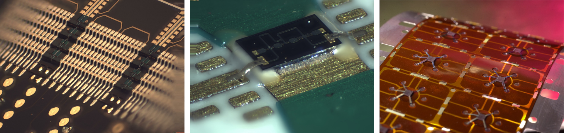
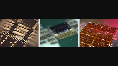
Semiconductor packaging examples showing printed 3D interconnects for 3D stacked die (l), mmWave (c), and flex circuit (r).
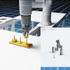
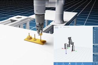
Optomec’s patented Aerosol Jet 3D electronics printers are an additive electronics solution uniquely capable of directly printing high-resolution conductive circuitry with feature sizes as small as 10 microns. The process is further differentiated by its ability to print onto non-planar substrates and fully 3D end-parts. Production applications include direct printing of 3D antennas, 3D sensors, medical electronics, semiconductor packaging and display assembly.
A primary high-value use case in semiconductor packaging is the printing of 3D interconnects to connect chips to other chips, traditional circuit boards and even directly integrated into end-products, such as wearables. In this case, the process replaces legacy wire-bonding due to its advantages in terms of smaller space claim, lower loss (especially in high frequency and mmWave) and greater mechanical reliability.